The Ultimate Spring Reverb Recovery Amp
Copyright 2003
Roy Mallory
In my tech note tech note I describe a simple and very good reverb recovery amp using a monolithic op amp and only a few components. However, it does not offer the ultimate in low-noise performance. Low-cost, JFET-input op amps generally have input-referenced voltage noise of from 8 to 16 nV/rt Hz in the middle of the audio spectrum, whereas discrete, inexpensive JFET transistors offer noise voltages of about 2 to 3 nV/rt Hz. In addition, some JFETS often have noise lower than what their data sheets specify. Therefore, this paper describes a composite op amp that uses a single JFET for its input stage. The basic circuit topology looks like this:
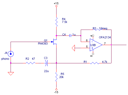
Figure 1
We see that the input (via phone jack J4) is applied to the gate of a JFET, and the output of the JFET goes to the inverting input of an op amp. The output of the op amp is fed back to the source connection of the JFET. The feedback connection combined with the high gain of the op amp acts to keep the current through the JFET constant. Another way to think about this is that the feedback forces the gate and source terminals of the JFET to track. This circuit is really just a non-inverting amplifier whose gain, in its pass band, is A = 1+ R2/R1, just like any other non-inverting op amp stage. One might wonder why I didn't use a differential pair instead of a single-ended JFET stage at the input of the op amp as is typically done. The answer is simple: in a differential pair, the noise of each JFET adds so as to increase the noise contribution of the JFETS by 3 dB. Of course, unlike a typical, differential-input, op amp stage, this circuit cannot respond down to DC. In fact, its low-frequency 3 dB point is defined by R2 and C3, and is
![]()
In the example above, Flow = 147 Hz.
Let’s look at some of the other components. R5 and R1 sets the current through the JFET, which, in this case, is about 1.25 mA. R4 is chosen to keep the drain of the JFET near the middle of the available voltage swing. R3 serves no other purpose other than to provide bias current for the op amp’s inverting input, and to keep the DC output of the op amp close to 0 volts. Its value should be large enough not to lower the gain of the stage, and 10 megs works nicely. C4 is made large enough not to influence the gain or low-frequency rolloff of the stage.
The JFET is chosen mostly for its low votage noise, but, of course, its break-down voltages limits, Idss, transconductance, and other parameters must be taken into consideration. I tested several readily available JFETS, and many proved suitable. The venerable PN4393 (or 2N4393) proved to have the lowest noise of any cheap JFET and is one of the easiest JFETS to find. The J310 is another good choice. There are some exotic JFETS with even lower noise that can be used. They will be discussed later.
There are a number of noise sources in this amplifier stage. First, is the Johnson noise of the real part of the reverb tank’s output impedance, which is just its DC resistance. For most of Accutronics’ tanks, this resistance is 200 ohms. The JFET’s voltage noise is multiplied by the signal gain of the stage, which, in the example, is 101. The FET’s current noise is multiplied by the input impedance of the reverb tank and the signal gain of the amp. Luckily, because the bias current of the FET is so low, this noise source can be ignored. The noise of the op amp also contributes, but it is divided by the gain of the JFET stage. The gain of the FET stage depends on the type of FET that is used, but for the PN4393, we can conservatively call it 40.
As usual, resistors contribute their Johnson noise. As is typical, resistor noise is modeled as a noise source in series with the resistor in question. R2’s noise is multiplied by the inverting gain, or 100 in the example. Both R4 and R5 contribute their noise. The easiest way to calculate their contribution is to note that the feedback loop acts to keep the current in the FET constant in the face of noise from R5. The output, acting through R1 accomplishes this. Therefore, the Johnson noise of R5 is multiplied by R1/R5, which, in the example, is about ¼. Similarly with R4, its noise is amplified by the ratio of R1/R5.
R1’s noise is amplified by one. In the case of R3, the output will swing to provide a current equal to R3’s voltage noise divided by R3. Therefore, the gain of R3’s Johnson noise is R1/R3. Let’s add up all these noise sources to see which are important, and what the total noise of the stage is. Remember that like all uncorrelated voltages, they will add in a root-sum-squared (r.s.s.) way. That is, each noise voltage must be squared, then summed, and the sum then square rooted.
|
Source of noise |
Output Noise (nV/ rt. Hz) |
|
Tank |
182 |
|
JFET (2.5 nV/ rt Hz voltage noise) |
253 |
|
R1 |
8.7 |
|
R2 |
87 |
|
R3 |
.19 |
|
R4 |
6.9 |
|
R5 |
4.2 |
|
Op amp (8 nV /rt Hz voltage noise) |
20 |
|
Total |
323 |
We see that the only two noise sources that are significant are the resistance of the reverb tank and the voltage noise of the JFET. R2’s noise could become significant, but by keeping its resistance substantially lower than the tank’s it is not an important contributor.
With the values and parts chosen, the total output noise is less than twice that contributed by the tank alone. If we wanted to use a more exotic JFET, Inter-Fet, http://www.interfet.com/ has several types whose voltage noise in the audio band is no more than 1 nV/ rt. Hz. If we used one of these FETS, the total output noise would be only 1.25 times larger than the noise of the tank. That’s awfully close to ideal.
So, are we done? Not quite. Like most single-ended gain stages, the JFET stage in this circuit is susceptible to power-supply noise. In addition, we need to discuss stability and how to limit the bandwidth of the circuit. It’s also worth discussing how to reduce ground-loop and common-mode noise. Below is a fully-developed circuit including components that deal with these issues.
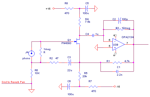
Figure 2
First, let’s discuss power-supply decoupling for the JFET. In the circuit above, the decoupling is accomplished by R8-C5 and R7-C6. These components introduce a pole at 3.4 Hz. Power-supply noise affects the circuit exactly like noise in R5 and R4. As we have seen, this noise is not amplified by the signal gain, but appears at the output as the ratio of R1/R5 and R1/R4 respectively. Therefore, it is not hard to filter out. One could replace R5 with a current source in order to suppress the effect of voltage noise on the negative rail, but current sources have their own noise, and the R-C filters are very simple and cheap.
Next, to frequency response and bandwidth limiting. The circuit is perfectly stable if C1 and C2 are removed. With them out, however, the bandwidth of the circuit is very broad, and because we’re not really interested in receiving A.M. radio stations, some response shaping is a good idea. One might think that adding C1 as would be done in an ordinary non-inverting op amp stage would be sufficient. However, adding this component reduces the signal gain at high frequencies, which also raises the loop transmission at those frequencies. (Loop transmission is defined as the forward open-loop gain of the circuit divided by its noise gain.) C2 adds some phase lead into the circuit, and that stabilizes it. The selection of C1 and C2 depend highly on the selected signal gain of the circuit, of course. With the components as shown, the stage has a high-frequency 3dB rolloff at 15 kHz, which seems appropriate.
Now, let’s talk about ground loops and common-mode noise. Reverb tanks are notoriously susceptible to magnetically induced hum, but because their output signal requires a lot of amplification, ground loops and common-mode noise can also be problems. Looking at the 2nd schematic, we see that J4, the connection to the tank is not connected directly to ground. Instead, a separate ground wire goes to the tanks’ metal shield. R6 provides a ground reference to the circuit when the tank is unplugged.
By floating J4, common-mode signals are only amplified by one, not by the signal gain of 101. Therefore, they are substantially suppressed. In addition, floating J4 breaks any ground loops. Note that if the reverb tank is conductively mounted to a grounded chassis, the extra ground connection to the tank should not be needed. Otherwise, it will be required.
Finally, I have built and installed the circuit shown in Figure 2 using the values and components as shown. It works just fine and is noticeably quieter than a conventional circuit using just an OPA134 op amp configured as shown in my tech note. The modifications used to reduce common-mode noise and ground loops were also effective, and the hum was also reduced. In fact, with the reverb gain set to a typical level, the reverb circuit is quiet and adds no audible noise to the overall amplifier, which is a claim that not many spring reverb circuits can make..